

Response Doctoral Program
Background
The unprecedented pace of technological progress is transforming our society, but is also driving an ever-growing demand for electrical energy. Meanwhile, The UN Sustainable Development Goal 7 pushes toward a future where everyone, everywhere, has access to clean, affordable, and reliable energy. This calls for cleaner production and conscious use of sustainable energy. Addressing this challenge of a sustainable energy transition is vital for the future of our society. A key factor in this regard is the efficiency of electrical networks. An efficient network, with minimal losses, enables innovations such as smart grids and the integration of renewable energy sources.
A critical component of electrical efficiency are power semiconductor devices. These devices are the backbone of electrical networks and are fundamental in many applications, including electric cars, data centers, and renewable energy systems. Traditionally, the most established power semiconductor devices have been made with silicon. However, increasing demands for performance and efficiency have pushed the requirements beyond silicon’s capabilities. In response, new materials known as wide-bandgap semiconductors (WBG) are taking over the market due to their superior efficiency.
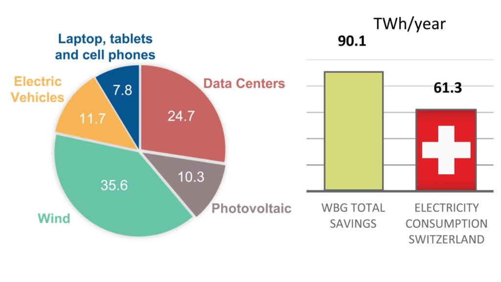
The estimated energy savings if we would adopt these materials across the main applications worldwide is shown in figure 1. In 2020, we could have reduced the worldwide energy use by 90.1 TWh/year. This is equivalent to 1.3 times the yearly electricity consumption of Switzerland. This was considering the size of the network and applications in 2020. However, the electricity consumption is only expected to grow. Therefore, the potential energy savings by integration of WBG technology will exponentially grow in the years to come.
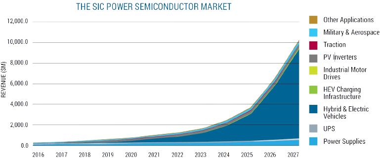
An exceptional semiconductor for new power devices is silicon carbide (SiC). The market projections for devices based on this material are outstanding, as shown in figure 2, placing it at the forefront of pursuing efficient and reliable energy systems. Manuel Belanche is a Doctoral researcher at the Advanced Power Semiconductor Lab (APS) at ETH Zurich, as well as a RESPONSE fellow in the PhD Program Science and Policy. He focuses on studying the physical properties of this material to help in the development of next-gen devices.
Next-generation material and devices
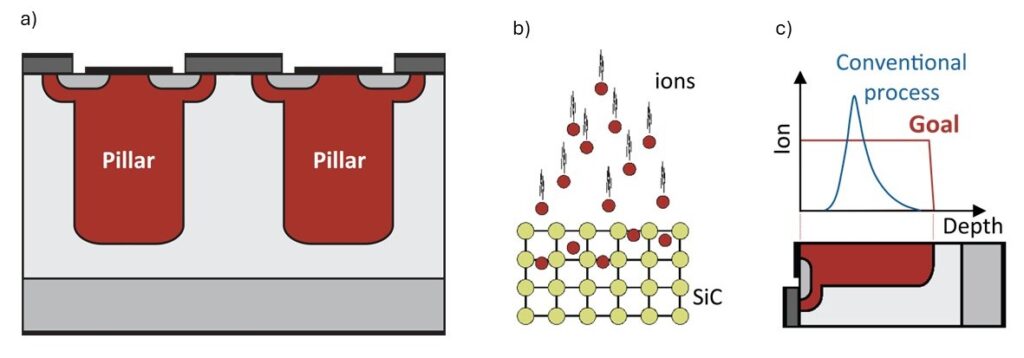
In addition to improving efficiency through innovative materials like silicon carbide, semiconductor devices can be further enhanced by re-imagining their design. One such innovative design is the super junction (SJ) structure. This design has demonstrated its benefits in conventional materials, promising a 20% reduction in energy losses. However, transferring this design to silicon carbide presents a significant challenge: fabricating the characteristic doping regions of a super junction structure, commonly known as pillars – shown in red in figure 3a.
A doping region is a volume in the semiconductor material populated with foreign ions, such as aluminum (Al). This step is essential in the fabrication of any semiconductor device. Particularly for SJ pillars, the ion population must be highly homogeneous and penetrate deeply into the semiconductor material. The goal is to develop a manufacturing process capable of achieving these SJ pillars in silicon carbide.
To do this, Manuel and his colleagues are using ion implantation, a well-known technique for creating doping regions in semiconductors. This technique consists of “shooting” ions into the semiconductor crystal at a defined speed, which allows controlling the distribution of these foreign ions within the crystal (figure 3b). Using the conventional approach, the ion distribution profile resembles the blue curve in the figure 3c. However, they are taking it one step further to achieve the required homogeneous and deep profile for the SJ pillars, illustrated by the red curve in figure 3c.

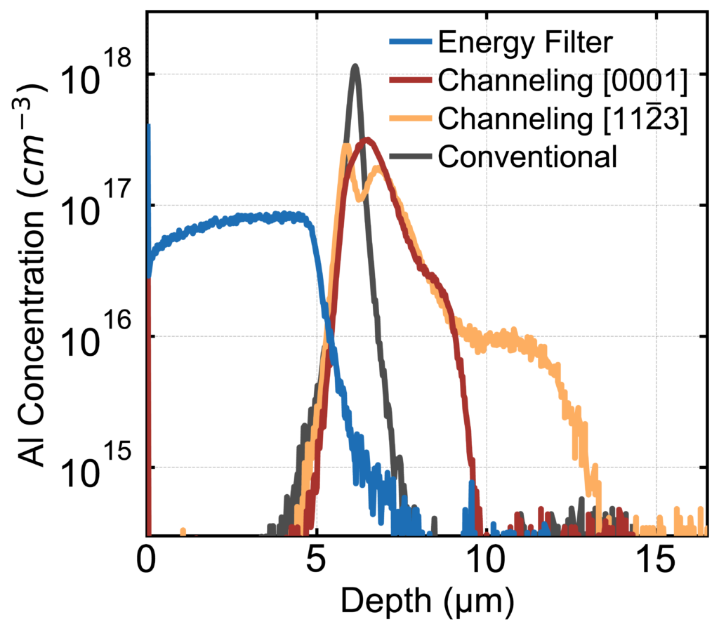
In his first publication, Manuel and his colleagues investigated two methodologies to achieve the required ion distribution. The first method consists of exploiting an interesting physical phenomena observed in crystals called ion channeling. This approach faces technical challenges that require an additional step to better understand the silicon carbide crystal. After addressing these challenges, Manuel and his team concluded that channeling implantations offer advantages for deep implantation and improved homogeneity.
The second method they explored was the ion implantation technology developed by their industry partner, mi2-factory, known as energy filtered implantations (see figure 4). Energy filtering achieves an outstanding homogeneity, while being more limited in deep implantation. This is illustrated in figure 5 (blue curve), in comparison with experimental results of channeling (red and orange curves) and conventional implantations (grey curve). The results so far indicate the potential for realizing devices that can enhance the efficiency and reliability of the overall electric grid.
Policy Relevant Research Outputs
This project bridges fundamental understanding and practical applications of semiconductor physics to enhance energy efficiency in electrical applications. Through advancements in materials and device design, we improve the efficiency of the energy system. Now, we need to facilitate the adoption of such efficient energy systems.
An example for policymakers on wide-bandgap semiconductor devices is the “Technology Collaboration Program on Energy Efficient End-Use Equipment” from the International Energy Agency. This initiative leverages international expertise to accelerate market entry. Additionally, key policy actions could include encouraging the adoption of wide-bandgap semiconductor devices by offering tax breaks and establishing efficiency standards to drive the market demand. This would also promote international collaboration among stakeholders in the energy sector.

Manuel Belanche is a fellow of the RESPONSE Doctoral Program (DP) «RESPONSE – to society and policy needs through plant, food and energy sciences» funded by the European Union’s Horizon 2020 research and innovation program under the Marie Skłodowska-Curie Grant Agreement No 847585.
This article is co-authored by Manuel Belanche and Mary Ann George (University of Zurich, RESPONSE Program office assistant).